
Array of Engineers Designs Custom SLVS-EC for FPGA Developers
- Jan 25, 2022
- 3 min read
Updated: Mar 16, 2022
Author: Brendan Grimes
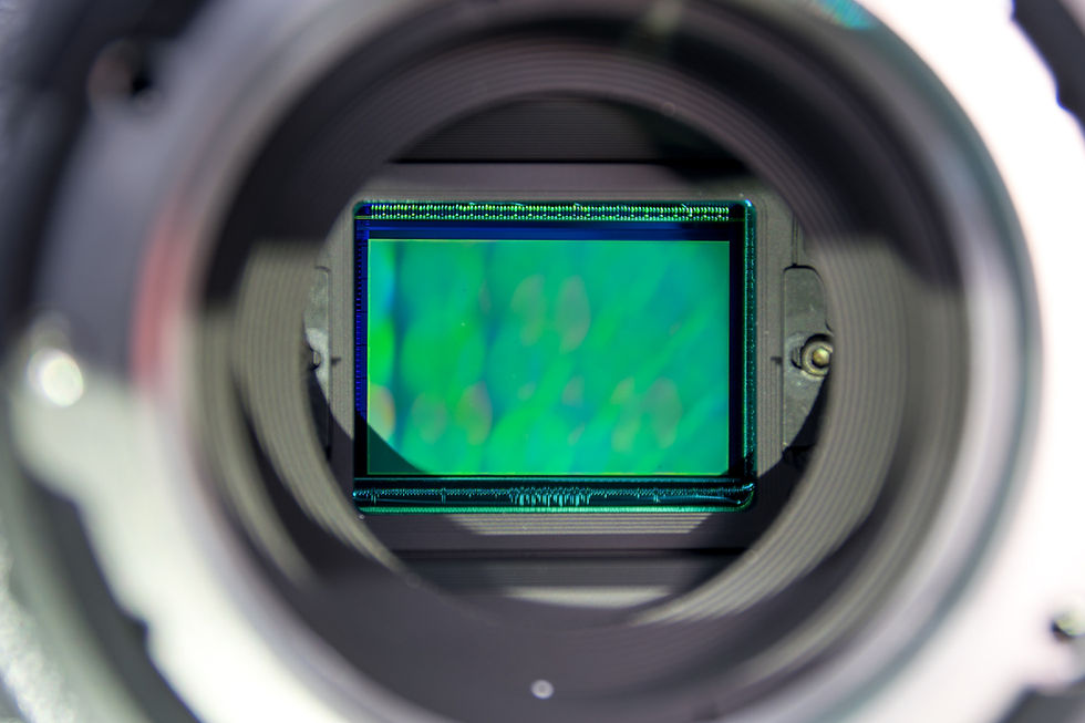
Array of Engineers is changing the game for FPGA developers using high-speed optical sensors. The research and development team at Array of Engineers has developed their own custom Scalable Low-Voltage Signaling with Embedded Clock (SLVS-EC) interface IP core. Our SLVS-EC IP core was written in Verilog and intended for use on any Xilinx SoC device that has high-speed serial interface lanes (GTX, GTH, GTY). The SLVS-EC standard, developed by Sony, has rapidly become the interface of choice for all high-end CMOS sensors - camera chips that convert light into electrical signals. The SLVS-EC interface standard makes a significant improvement in data throughput over longer distances, as compared to conventional uncoded SLVS and LVDS interfaces. Where conventional SLVS interface speeds may only reach ~600 Mbps per lane, SLVS-EC can provide throughputs of up to 5Gbps per lane. In addition, the SLVS-EC does not require the use of a separate clock lane, as the clock signal itself is embedded in the data stream itself.
Many Sony camera chips now only support the EC interface. We are also starting to see other imaging sensor suppliers use the EC as their own standard as well. Therefore, the SLVS-EC IP core that Array of Engineers has developed enables us and our partners to leverage the latest integrated circuit imaging technologies in our FPGA designs. Unfortunately, access to such an IP core for FPGA developers has been severely limited, with single-source supply being a chief problem. Array of Engineers hopes to resolve this by making the challenge of implementing high-end imaging sensors on FPGA designs less daunting and more accessible. With our new SLVS-EC FPGA core, FPGA developers now have another source of expertise they can leverage for their FPGA programming projects.
One of the most challenging problems the firmware design team at Array of Engineers faced in the development of this IP core was writing the combinatorial logic for the data/clock deinterleaving process itself. Camera frame deinterleaving is the process of dicing pixel frame data onto multiple lanes. This helps distribute the data transitions more evenly across lanes and embeds additional data in the data stream. While the Xilinx GTH transceiver cores are easily configurable and can automatically implement the 8b10b line coding, the image frame data deinterleaving across all 8 lanes was implemented directly from scratch, using only the protocol data sheet as a reference. However, with systematic and persistent code development and extensive testing, our team was successful. While AoE’s development project for this IP core was geared toward use with the Sony IMX-426 Pregius camera chip, it is highly configurable and can be used with any SLVS-EC device. Leveraging our SLVS-EC IP core for an optical sensor FPGA project ultimately enables:
Seamless addition of latest SLVS-EC sensors into Vivado
Tested and validated embedded FPGA logic
Reduced FPGA development timelines
Specific support for IMX-426 camera chips
To learn more about Array of Engineers’ FPGA designs and current lineup of additional IP cores, including our AXI CAN, AXI DAC Driver, AXI SPI Master, and AXI I2C Master core, check out the AoE products page. Feel free to reach out to us via our website or on LinkedIn.
Brendan Grimes is the Vice President of Hardware & Firmware at Array of Engineers, where he leads research and development for FPGA engineering, PCB prototyping, and hardware development. Brendan has 15 years of engineering experience, with extensive expertise in embedded software & firmware.


Comments